This is a VHDL implementation of the project described at Zimmers website (the files in 251715.zip). The original project used a combination of a TDF file (Quartus Text Design File, looks a bit like Abel, with & for AND, # for OR and ! for NOT and the same operator precedence as in Abel) for the PLA chip, which was used in older C64 models, and two Quartus schematics entry files, to model the new chip used in newer C64C models (see C64 Wiki for details), which integrates the old PLA chip and some of the surrounding support chips in one big 64 pins chip. See the readme of the original project for the details of the project and author credits.
You can find all VHDL sources, the Eagle files and the old project files at my GitHub repository. Most of the VHDL implementation was written by Jani Kuituniemi, who learned VHDL with this project, check out his blog and plans to implement a better BASIC for the C64 and a turbo mode for the 6510. On GitHub the original design is on the "gates" branch. On the "master" branch I've implemented a simpler, more high-level description of the hardware.
First I converted the C64PLA7.TDF file. It was just a bunch of logic functions and an output enable pin, which switches all outputs to tri-state, which I basicly could translate with text replace and adding some parantheses, because in VHDL the AND and OR operators have the same precedence.
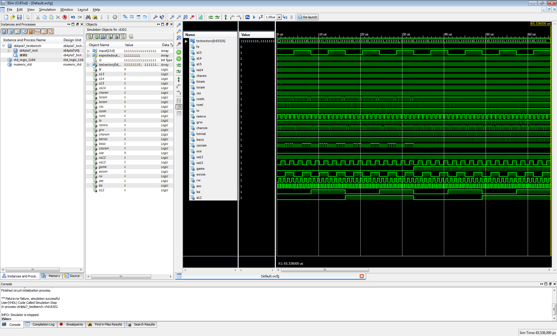
For testing the implementation, I've created a VHDL test bench. There is a C program at zimmers.net, which is used to create the data for an EPROM for repairing broken old PLAs and which generates all possible input/output combinations of the chip. I modified it to create a test vector, which I copied to in the test bench c64pla7_testbench.vhd.
isim has a limit of 65,536 elements per object, but the test vector requires 524,288 elements, which can be changed with "isim set maxtraceablesize". To set this automaticly at startup, you have to create your own isim.cmd file. Usually the file "isim.cmd" is used. I created a file my-isim.cmd with the content of isim.cmd and the trace limit line added:
isim set maxtraceablesize 1000000
onerror {resume}
wave add /
run all;
and specified this in Process Properties (right click "Simulate Behavioral Model", click "Process Properties", select "Use Custom Simulation Command File" and specify the file in "Custom Simulation Command File"). The last line of isim.cmd was "run 1000 ns;", which I've changed to "run all;". This means it runs for an unspecified amount of time, in this case until the loop is finished and the last command, "assert false report "no failure, simulation successful" severity failure;" is executed, which stops the simulation at the end (if there are some clocks in infinite loops simulated, it might run forever otherwise). This works for other simulators, like ModelSim, and more complex test benches as well.
This is how it looks like in isim:
When programmed in a CPLD, it can replace the 28 pin PLA 906114, e.g. used in C64C models with PCB assembly number 250466.
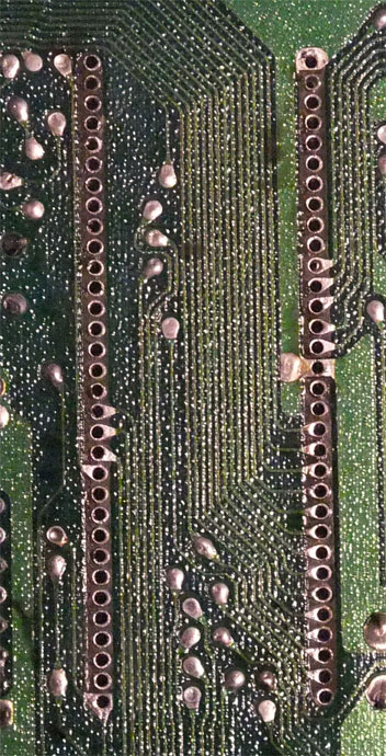
These are the schematic diagrams of the new 251715 PLA used in newer C64C models (with PCB assembly number 250469) is a 64 pin chip, as implemented with the two Altera CPLDs in the original project: chip1.pdf, chip2.pdf . And in some of the latest models there is a 252535 PLA, with integrated color RAM.
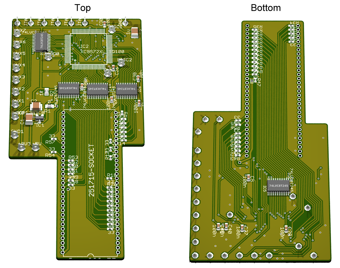
Ported to a XC9572XL and created an Eagle schematic and board. Eagle 3D preview:
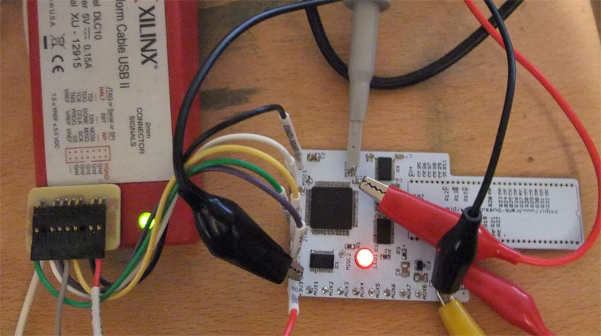
The PCB arrived, I've soldered the CPLD and uploaded a blinking program:
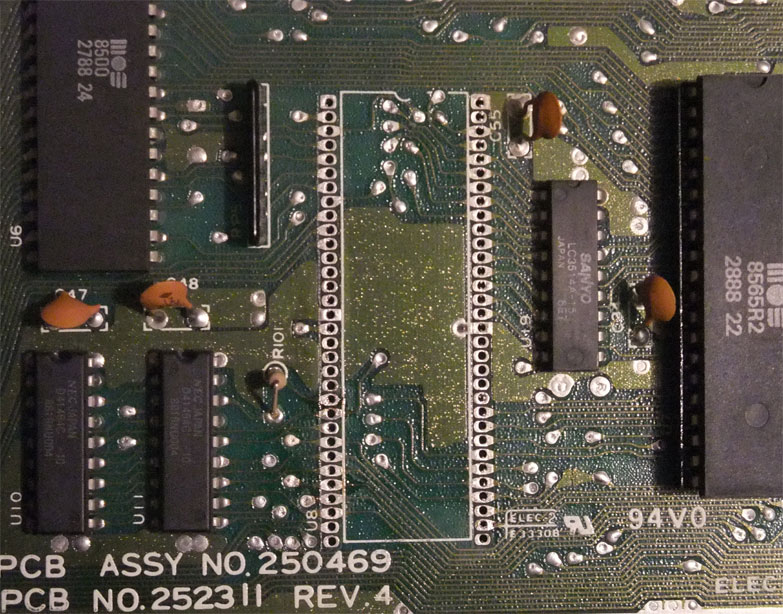
I've desoldered the PLA in the C64 with a ZD-987 vacuum desoldering station to remove most of the solder for each pin, and then heated up the residual solder with a AOYUE 998 hot air station which made it easy to remove the IC with a screwdriver and pliers. After cleaning the holes with some solder wick, the top of the C64 PCB looks like this:
and the bottom:
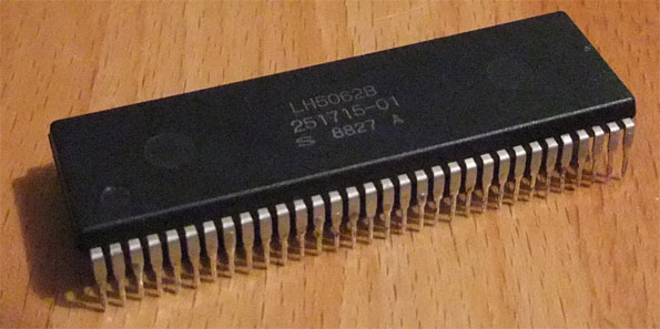
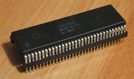
The C64 PLA chip, after cleaning the pins:
For soldering the new socket rows, it was easier to insert the chip into the rows first:
and then inserting both into the C64 PCB:
After soldering, I removed the PLA and inserted the pin headers:
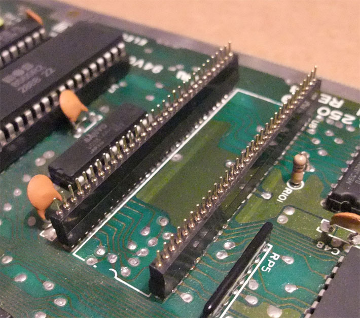
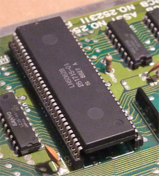
Then I inserted the new PLA implementation PCB and soldered it:
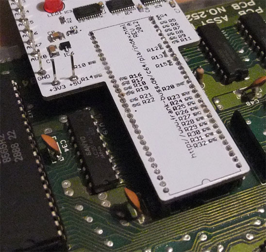
Now I can use the old PLA chip or the new implementation.
First there was a major hardware bug: The VIC requires to switch ma0-5 to input and ma6-7 to output, which is not possible with just one 8 level voltage level shifter as I planned it. Fortunately the RAM chips are working with the 3.3V output from the CPLD without voltage shifting. That's again the time when a hot air station is useful for desoldering the TSSOP voltage level shifter chip and a microscope for soldering some wires:
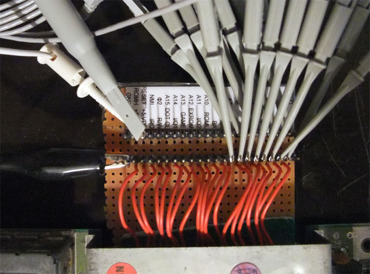
But there was another problem: The CPU read the reset vector, but didn't jump to it. The reason was that I forgot a "not" for the AEC signal. Debugging was not difficult with a 16 channel logic analyzer. For easier debugging I built a breakout cartridge board for the expansion port:
This is how it looks after reset, after fixing the AEC problem. Yellow is reset and green is AEC:
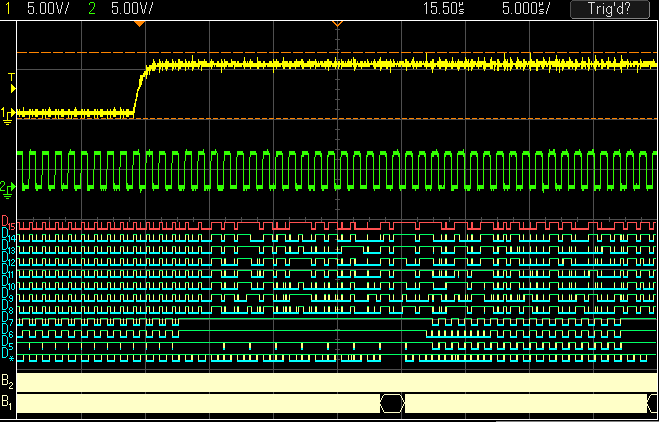
Zooming into the interesting part where it loads the reset vector and jumps to it:
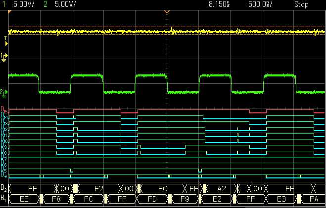
Bus B1 is the lower 8 bits of the address bus and bus B2 is the data bus. You can see that it reads the addreses $FFFC and $FFFD (the CPU accesses the bus always when AEC is 1), which reads the reset vector $FCE2 and then it jumps to it. The program at $FCE2 starts like this:
fce2   A2 FF      LDX #$FF
fce4   78         SEI
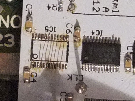
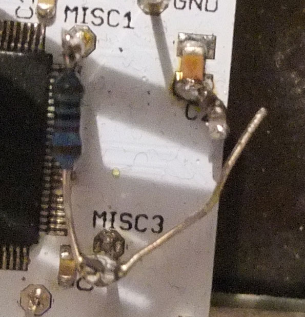
But the RAM still didn't work. One problem was the CASRAM delay, as described by Thomas Giesel in detail in his great documentation The C64 PLA Dissected and where you can learn how to decap a PLA with rosin, too. I added a RC delay element with two of the misc pins (always a good idea to add some misc pins to your circuits), outputting the CASRAM signal on MISC1 with a resistor to MISC3 and optionally a capacitor to GND from MISC3:
With a 47 pF capacitor the CAS to CASRAM delay was about 50 ns, which was too much, but without a capacitor, so maybe just the parasitic capacitance and the extra delay because of the additional output/input, the delay was about 20 ns.
But it still didn't work, maybe because of problems with my implementation of the low-level implementation of the gates from the schematic entry design from the original Quartus project. So I rewrote it from scratch, but this time in high-level VHDL, which describes the ideas how CAS/RAS works for accessing the RAM and how the CPU and the VIC shares the address bus much better, at least for me as a programmer. The new source: c64pla_251715.vhd. With this code it booted and I could see the usual start screen. There were some minor problems, like that I forgot to select the color RAM when the VIC owns the bus, which caused a nice color animation on the startup screen like this:
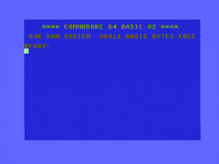
But after fixing this it worked! I'm sure there will be more problems when I try to use some cartridges or play some games with it.
For some more testing I've added a function to turn on the LED on the PLA board when accessing the memory at IO1 ($DExx) and to turn it off for IO2 ($DFxx). My first implementation was to change the LED at the same time when IO1 or IO2 is set to low. This didn't work, because of glitches on IO1 and IO2 when the address bus is not stable: Sometimes the LED was turned on, but some milliseconds later turned off again, sometimes it was turned on on its own. There is not much logic on the CPLD to implement a clean delay with a higher frequency oscillator and I didn't want to implement another external RC delay, but turns out that using the falling edge of CAS for sampling IO1 and IO2 is very reliable. A "POKE56832,0" from Basic turns the LED on and "POKE57088,0" turns it off all the time.
After some more debugging from Jani and me, the "gates" version in GitHub works now, too. Was just a minor problem in the multiplexer. Remember: use always testbenches.
