Finally the ROM emulation is working, running at 1 kHz, which is also generated from the PIC, just in time for the end of the Retrochallenge Competition (not really a competition, but a fun event, challenging yourself to at least finish your retro-style project). With this circuit I can test now programs for my 4004 CPU with fast turnaround time, by just flashing a new program to the PIC.
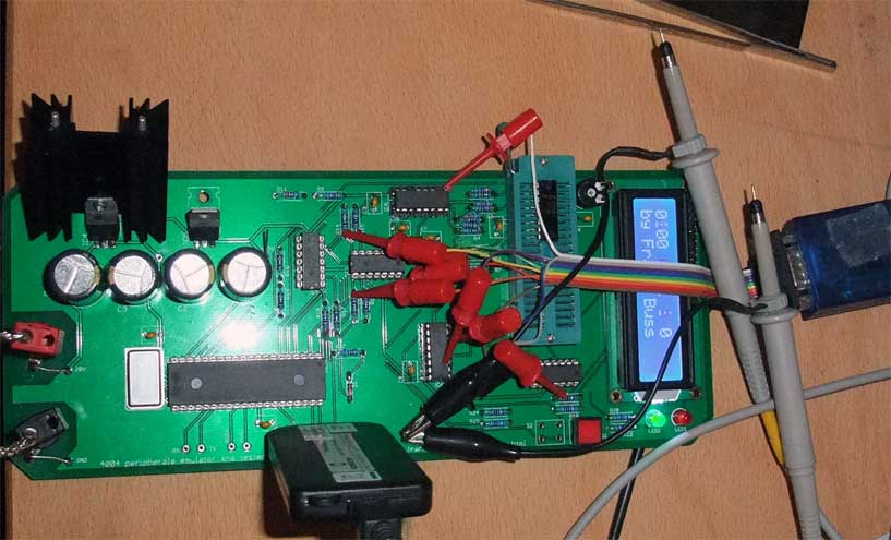
The ZIF socket looked so empty, so instead of emulating a RAM or the out ports from the ROM with the PIC and showing the state in the display, as planned at the beginning of this project, I've added another chip from the MCS-4 family, a 4002 RAM with some wires, and four LEDs. Now the LED test program from the beginning of this month works without modification:
The source code, updated Eagle schematic and layout files and the final schematic as PDF.
I've modified the circuit a bit more: added enable data out pull-down, to set the output drivers to tri-state, and a reset pull-up, to hold the 4004 in reset while the PIC is booting. Then I implemented the ROM emulation with this program:
0000:        NOP             00
0001:        NOP             00
0002:        NOP             00
0003:        NOP             00
0004:        JUN $0000       40 00
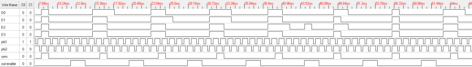
Of course, it didn't work the first time, because I missed that all inputs to the 4004 CPU are inverted, except the two clock inputs, which already worked. After fixing this, it still didn't work, because the input impedance was really low, so I soldered 220 ohm resistors in parallel to the 10 k series resistors for D0-D3. And now it works, this is a screenshot of my Ant8 logic-analyzer:
You can see how the address request from the 4004 CPU is counting up on D0-D3, just after the sync signal, from 0 to 5 and then back to 0. It works down to 10 Hz. With 5 Hz it counts just until 3, then resets to 0. So I generate 1 kHz from the PIC, which should provide some safety margin. Maybe later I'll port it to a FPGA, to run it with the full 750 kHz.
I've soldered some wires to the IC pins for the logic analyzer clips. Next time I'll add more test points :-)
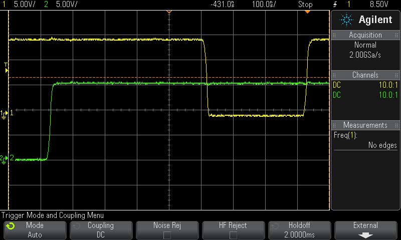
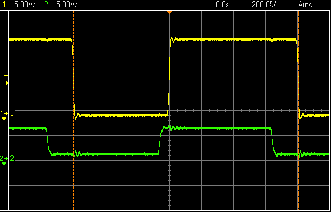
When measuring the clock, sync and data signals with my scope, you can see when the data lines are going to tri-state:
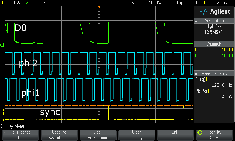
It looks like the CPU is enabling data output for the X1 cycle (see datasheet of the 4004 for a description of the cycles) with falling edge of phi1, until rising edge of phi2. And looks like the address at A1 is set with rising edge of phi2, which is the reason my PIC program samples it with the next rising edge of ph1, because then the signal should be stable, I hope.
I guess I do enable the output driver to the CPU a bit too early, because the CPU might sample the data bus with the rising edge of ph1, so I could enable it with falling edge of ph1 and disable it a bit earlier, too.
BTW: the trick to have 4 traces on the scope with a 2 channel scope is to use the "Capture Waveform" function, move the y-position of the trace, capture again etc. But works for repetitive signals, only.
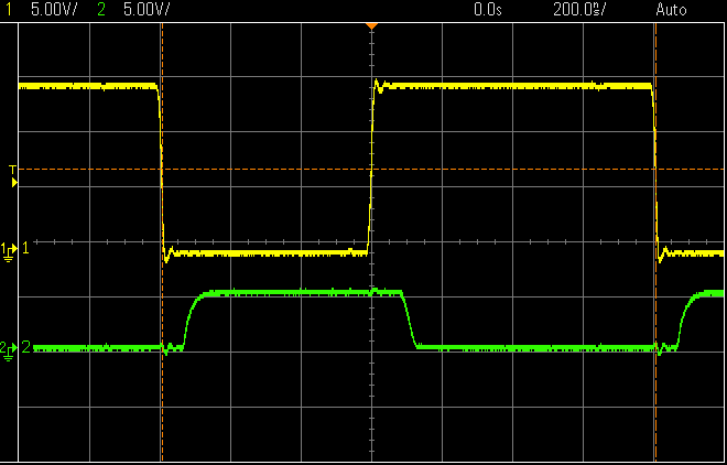
The 4004 is alive! The yellow and cyan traces are the phi1 and phi2 signals, generated by the PIC and the green signal is the sync response, generated by the 4004 CPU:
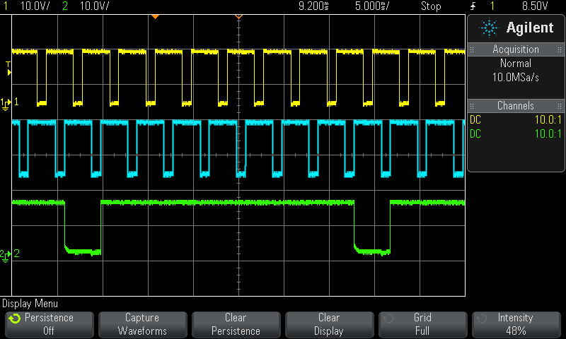
I had to remove the 10 k series resistors for phi1 and phi2, because the rise and fall time was too slow, but it is not needed anyway. This is a detail scope image of the clock signals:
More than twice as fast as tested on my breadboard.
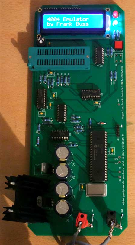
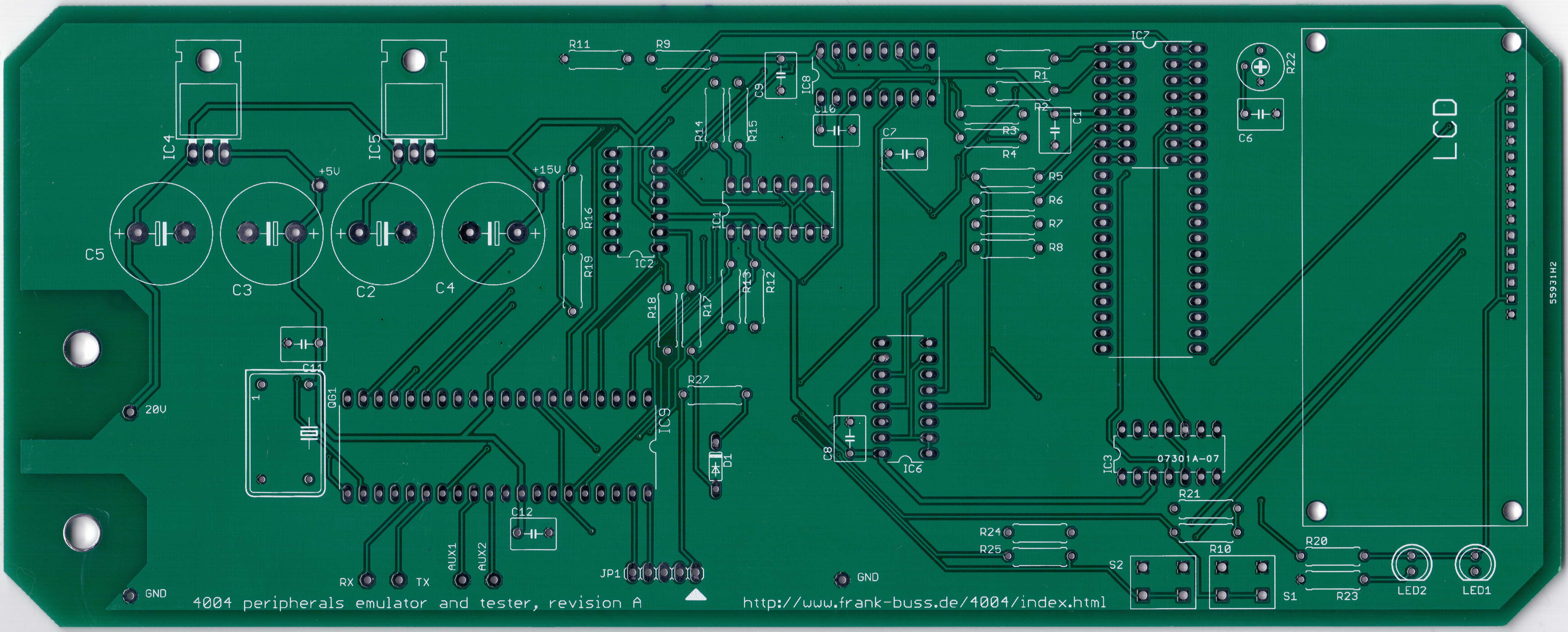
I got the PCB today (I ordered it 11 days ago from ITeadStudio, shipping with UPS is really fast), very good quality. All components are soldered, after fixing the problem with the wrong footprint for the trimmer with some wires. The 5 V linear regulator gets a bit hot, because I need 20 V for the 15 V regulator and currently it needs 100 mA, but with a big heatsink it gets just lukewarm. Another problem is with the green LED: it is not easy to see because of the illumination of the display backlight. Maybe I should use some electrical tape, if it doesn't get too hot. The PIC16F887 is working and I can show something on the display and the red LED is blinking. Now the fun starts: writing the emulator for the peripherals of the 4004 and verifying the signals in single step mode (with the key), then placing the 4004 in the ZIF socket.
The instruction set of the Intel 4004 is a bit complicated for accessing external chips, but it is not as bad as PIC assembler. There is a nice assembler and emulator at http://e4004.szyc.org, with which I've compiled my first 4004 assembler program, a LED Knight Rider effect: Intel 4004 LED test program (source code) . Another awesome gate-level simulator: http://www.4004.com/mcs4-masks-schematics-sim.html#simulator. The next step is to write the PIC program for emulating the ROM. For the RAM I've bought an original 4002-1 chip from eBay, I should get it next week.
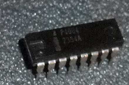
I've bought a P4004 from eBay:
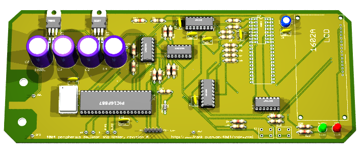
My idea is to emulate the peripheral chips like the 4001 ROM, to run some programs on it. So far I've designed the schematic, placed the components and used the Eagle auto-router. The current Eagle files: eagle.zip. The board will look like this:
I measured the propagation delay of the level shifters and should be ok. It is less than 200 ns for the 40109:
and for the 339 comparators:
The 4004 works only up to 700 kHz, so should be sufficient.
